Scanning Electron Microscopy: SEM
Scanning Electron Microscopy SEM
Devices
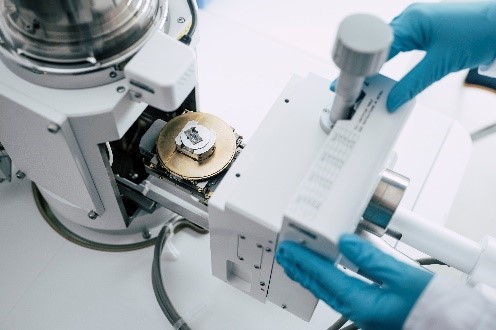
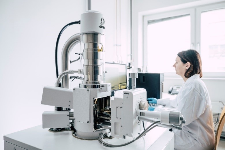
JSM-IT 100 / JEOL
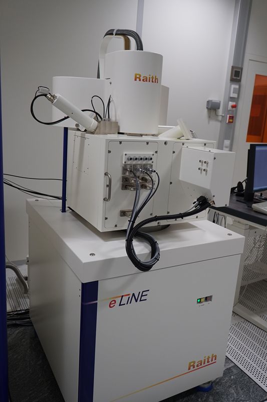
e-line / RAITH
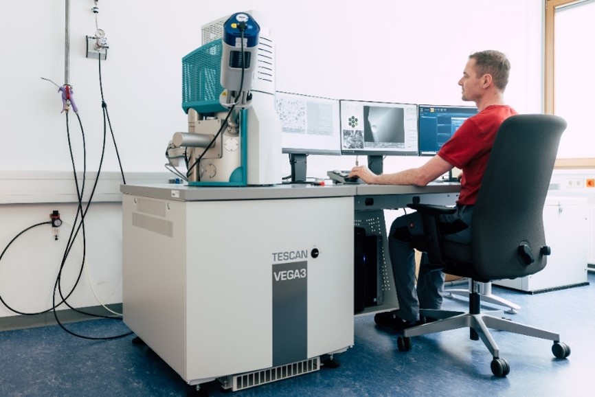
Vega 3 / TESCAN
Expected Result
High resolution images of the nanostructure, particles and surfaces. EDS option: enables precise analysis of chemical properties, essential for understanding material composition and arrangement. EBL option: Fabrication of structured surfaces from nm - µm dimensions.
Method
High-resolution imaging with the options of chemical element analysis by energy dispersive X-ray spectroscopy (EDS) and electron beam (e-beam) lithography (EBL).
Case Study
A customer in material science requires detailed imaging and compositional analysis of a multilayer metal coating. The SEM captures high-resolution images of each layer’s topography, while EDS detects the elemental composition, revealing differences in the distribution of metals across the layers.
Scanning Electron Microscope SEM JSM-IT 100 / JEOL


Specifications
- Maximum sample size: diameter 80 mm, height 35 mm
- Sample loading and unloading time: ≤ 4 minutes
- Resolution: nominal (diam. e-beam) 4 nm, in practice features down to ≈100nm resolved (reasonable magnification x30.000 at 128 mm x 96 mm image), depends heavily on sample. Requests of customers are checked individually.
- Accelerating Voltage: 0.5 to 20 kV
- Sample manipulation (stage): tilt -10° to 90° ; rotation 360° ; movement: 80 x 40 mm
- Low vacuum option for non-conductive / out-gassing samples
Vega 3 SEM + AZtec Energy-Dispersive X-ray Spectroscopy (EDX)

Specifications
- OXFORD INSTRUMENTS AZtec energy dispersive X-ray spectroscopy detector (EDX)
- Heated tungsten filament cathode
- Wide Field Optics™ Technology with Intermediate Lens™ and In-Flight Beam Tracing™
- Resolution:
- High Vacuum Mode: 3 nm at 30 keV. 8 nm at 3 keV
- Low Vacuum Mode: 3.5 nm at 30 keV with BSE detector
- Maximum Field of View: >50 mm at max WD
Chemical element analysis by EDS (~0.1 wt.-% for sodium and heavier elements)
Scanning Electron Microscope SEM e-line / RAITH

Specifications
- Max. sample size: 100 mm × 100 mm (4” wafer) on flat sample holder, 20 mm × 20 mm on tiltable / rotatable stage
- Max. sample height: 20 mm
- Max. acceleration voltage: 30 kV
- Resolution: < 5 nm
- Sample manipulation (RT stage): tilt up to 92° ; rotation 360°
- Emitter type: Thermionic (tungsten emitter)
Surface needs intrinsic conductivity or will be coated (Au, W)
E-beam lithography option
